PCB & Electronic Assembly: A Complete Guide

Get a FREE Product Sample Box!
Order a product sample box to feel the quality of our work before deciding to make a batch order.
At the core of nearly all electronic devices lies a printed circuit board (PCB). From simple household gadgets to complex industrial machines, these boards connect components, bringing the devices to life.
Printed circuit boards serve as the backbone for countless electronic devices, ranging from smartphones and computers to medical equipment and automotive systems. Regardless of size, every electrically powered device relies on some form of PCB to function.
Whether it’s a cell phone, a remote control, a complex computer, or a simple child’s toy, a PCB provides connectivity between all components of a device. As a result, the device will function as it should.
Explore the fundamentals of printed circuit boards as we delve into their structure and function, as well as unravel the mystery of how these boards operate.
Key Takeaways:
- PCBs connect and power components in nearly all electronic devices, from smartphones to industrial machines.
- From early point-to-point wiring to modern HDI, flexible, and multi-layer boards, PCBs have continually enabled smaller, faster, and more reliable electronics.
- Printed circuit boards support complex circuitry in small spaces while ensuring durability and precision.
- Proper design, testing, and manufacturing prevent failures and ensure long-lasting performance.
- Consider everything from capabilities to communication when choosing a manufacturer to ensure high-quality PCBs.
What Are PCBs?
At its core, a PCB is a flat board made of non-conductive material, typically fiberglass-reinforced epoxy laminate, with conductive pathways etched or printed onto its surface. Electrical components are soldered onto the PCB using either wave soldering or selective soldering. Then, a conformal coating is applied to protect the surface and secure its longevity.
The primary purpose of printed circuit boards is to provide a reliable platform for interconnecting electronic components compactly and efficiently. By guiding electrical signals through predefined pathways, PCBs ensure that electronic systems function with precision and reliability.
Types of Electronic Assemblies
Electronic assemblies come in several forms, depending on the level of integration, complexity, and support required for the final product. The three most common types are PCB assembly, turnkey assembly, and box build assembly. Each plays a critical role in bringing an electronic device from concept to completion.
PCB Assembly (PCBA)
Printed Circuit Board Assembly is the foundation of any electronic product. It involves mounting electronic components, such as resistors, ICs, and capacitors, onto a bare circuit board using surface-mount (SMT), through-hole, or mixed technology.
PCB assemblies act as the brain of an electronic device, enabling signals to flow and functions to operate. This stage focuses on precision, testing, and reliability, ensuring the core circuitry performs flawlessly.
Turnkey Assembly
Turnkey electronic assembly provides an end-to-end solution where one manufacturing partner manages the entire process:
- Component sourcing
- PCB assembly
- Testing
- Integration
This option reduces production time, minimizes vendor coordination, and lowers the risk of supply chain issues. Turnkey services are ideal for companies looking for a streamlined, cost-efficient path from design to finished electronics without juggling multiple vendors.
Box Build Assembly
Box build assembly, also known as systems integration, takes electronics beyond the circuit board and completes the full product enclosure. This can include cable harnesses, sheet metal fabrication, firmware installation, and product labeling, all the way through to final functional testing and packaging.
Box builds deliver a production-ready device that is fully enclosed, protected, and ready for shipment or deployment.
The History of PCBs
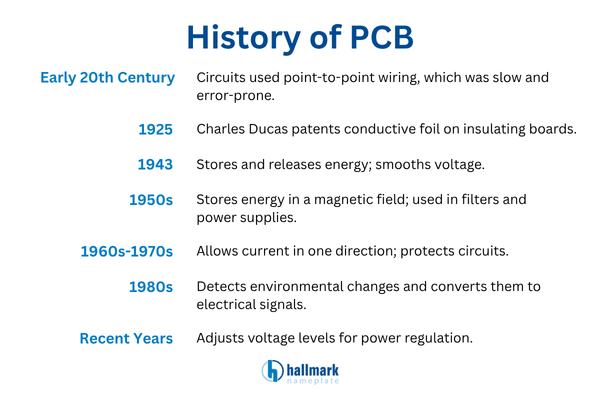
The origins of printed circuit boards can be traced back to the early 20th century. Before the invention of PCBs, electronic circuits were constructed using cumbersome and unreliable methods such as point-to-point wiring and terminal strips. These methods were labor-intensive and prone to errors and failures, so innovation was necessary.
Early Development
The concept of the printed wiring board, which became the modern PCB, emerged in the early 20th century. In 1925, Charles Ducas patented a method that used conductive foil patterns on an insulating board to connect electronic components, laying the foundation for PCBs.
World War II intensified the need for efficient electronic systems, leading Austrian engineer Paul Eisler to create the first true PCB in 1943. Eisler’s “printed wiring” invention was used in proximity fuses for Allied anti-aircraft shells.
Evolution of Printed Circuit Boards
Following World War II, PCB technology continued to evolve rapidly. The introduction of new materials and manufacturing processes led to significant improvements in PCB design and performance.
1950s
One of the key milestones in the evolution of PCB technology was the development of the ‘through-hole’ method in the 1950s. This method involved drilling holes in the PCB substrate and inserting component leads through the holes before soldering them in place. The through-hole method allowed for more secure connections and improved reliability compared to earlier methods.
1960s-1970s
In the 1960s and 1970s, the introduction of automated assembly techniques such as wave soldering and surface mount technology (SMT) revolutionized PCB manufacturing. Surface-mount technology, in particular, allowed for smaller and lighter electronic devices by eliminating the need for bulky through-hole components.
1980s
The 1980s saw the widespread adoption of computer-aided design (CAD) software for PCB design, further enhancing the precision and complexity of PCB layouts. This era also saw the emergence of multi-layer PCBs, which allowed for denser component placement and improved signal integrity.
Recent Years
In recent years, advancements in science, manufacturing processes, and miniaturization techniques have continued to drive innovation in PCB technology. High-density interconnect (HDI) PCBs, flexible PCBs, and integrated passive devices (IPDs) are innovative advancements expanding printed circuit board capabilities.
As you can see, PCBs have played a vital role in shaping the modern world of electronics from its humble beginnings to modern cutting-edge technology. Now, let’s discuss the importance of these electronic boards in our modern world.
The Importance of Quality PCBs
PCBs are essential to the electronics industry, powering virtually every electronic device. Here’s why they’re indispensable:
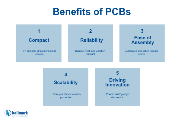
1.) Compact Design
One of the most remarkable aspects of PCBs is their ability to accommodate complex circuitry within a compact form. As devices become smaller and more powerful, PCBs allow engineers to pack an increasing number of components into limited spaces without compromising functionality.
From sleek smartphones to wearable fitness trackers and autonomous vehicle control systems, PCBs enable miniaturization, pushing technological boundaries.
2.) Reliability
Unlike the fragile, hand-wired connections of early electronics, modern PCBs are engineered for durability and precision. Advanced manufacturing techniques ensure that each PCB is produced with exacting standards, reducing the risk of electrical failure.
Their layered structure, reinforced with protective coatings, allows them to withstand extreme temperatures, vibrations, and moisture, making them indispensable in industries such as aerospace, healthcare, and industrial automation.
3.) Ease of Assembly
PCBs streamline the production process, eliminating the complexities of manual wiring and drastically reducing the risk of human error. Through automated assembly techniques like surface-mount technology (SMT) and wave soldering, manufacturers can produce electronics faster, more accurately, and at a lower cost.
This efficiency is crucial for mass production, ensuring that devices are built quickly while maintaining high quality.
4.) Scalability
PCBs provide a flexible foundation that can be scaled for any application. Whether designing a one-off prototype or manufacturing millions of units, PCBs can be customized to different shapes, sizes, and functionalities.
Engineers can develop multilayered boards for high-performance computing or flexible PCBs that bend to fit wearable technology. This scalability ensures that PCBs evolve alongside the needs of emerging industries.
5.) Driving Innovation
PCBs don’t just power today’s electronics; they shape the future of technology. Engineers and product designers rely on PCBs to develop cutting-edge innovations, from quantum computing to next-generation medical implants.
With advancements in materials, 3D-printed PCBs, and integrated smart technologies, the possibilities for what PCBs can enable are virtually limitless.
How Does a Printed Circuit Board Work?
Now that we have some background on PCBs, let’s dig deeper. PCBs might seem simple, but they’re crucial in directing electricity to power a device. These boards use layers of resin and soldered pathways to guide electrical signals, connecting all components and allowing the device to operate as intended.
Beyond powering the device, PCBs also provide a sturdy foundation for all components to attach. This makes them essential for both structure and function. In many ways, they’re the “brains” behind electronic devices.
So, let’s take a look at the components of a printed circuit board.
Components of a Printed Circuit Board
Understanding the components of a PCB is crucial for designing and manufacturing reliable electronic devices. By selecting the appropriate substrate materials, conductive layers, and solder mask materials, engineers and manufacturers can ensure the performance, reliability, and longevity of the final product.
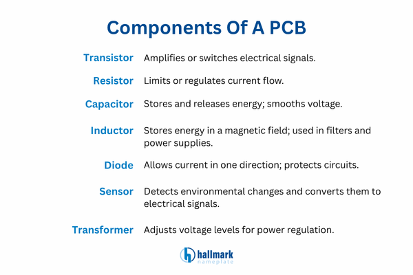
Most PCBs contain the following components:
Transistor
A transistor is a semiconductor device used to amplify or switch electronic signals and electrical power. It is one of the fundamental building blocks of modern electronics and plays a critical role in PCBs.
Resistor
Resistors are passive electrical components that limit or regulate current flow within a circuit. They are essential for ensuring that other components receive the appropriate amount of power without damage.
Capacitors
Capacitors store electrical energy temporarily and release it when needed. They help smooth out voltage fluctuations and improve power stability in circuits.
Inductors
Inductors are passive components that store energy in a magnetic field when electrical currents flow through them. They are commonly used in power supplies and filters.
Diodes
Diodes are semiconductor devices that allow electrical currents to flow in one direction while blocking them in the opposite direction. This makes them crucial for rectification and signal protection.
Sensor
Sensors allow a PCB to interact with the environment by detecting changes in temperature, light, motion, pressure, and more. They convert these physical inputs into electrical signals that a microcontroller can process.
Transformer
Transformers adjust voltage levels by either increasing (step-up) or decreasing (step-down) electrical energy. They are essential for power regulation and isolation.
Key Considerations When Creating PCBs
Designing a high-quality PCB involves more than just connecting components; it requires careful attention to the materials, layers, and protective elements that make the board functional and reliable.
From the substrate that forms the board’s foundation to the conductive copper pathways and protective solder mask, every element plays a critical role in performance, durability, and manufacturability. Understanding these key considerations helps engineers and designers create PCBs that meet the demands of their intended application.
Substrate Materials
Printed circuit boards (PCBs) use various substrate materials, which form the board’s base and support the components. The choice of substrate depends on factors such as the application, operating conditions, and cost. Some common types of substrate materials include:
- FR-4: One of the most common substrate materials is FR-4, a fiberglass-reinforced epoxy laminate known for its electrical insulation, mechanical strength, and flame resistance.
- Flex: Flex PCBs, made from flexible materials like polyimide or polyester, can bend to fit specific shapes and are ideal for applications like wearable devices and medical implants.
Conductive
Conductive layers are the metallic pathways on a PCB that provide electrical connectivity between components. These pathways are typically made of copper and are deposited onto the substrate using various techniques. Two key components of the conductive layers are:
- Copper Foil: Copper foil forms the conductive pathways on a PCB, and manufacturers typically laminate it onto the substrate using heat and pressure. This forms a thin copper layer that follows the desired circuit pattern, selected for its excellent conductivity and ease of fabrication.
- Copper Plating: Additionally, copper plating is applied to the walls of plated through-holes or vias to ensure electrical continuity between layers. This plating strengthens connections and is achieved through electroplating, where copper ions are deposited onto exposed surfaces of the PCB.
Solder Mask
The solder mask is a protective layer applied to the surface of the PCB, covering the conductive traces and pads while leaving the soldering areas exposed. It serves several important purposes:
- Purpose: The primary purpose of the solder mask is to prevent unintended electrical connections between adjacent traces or components during soldering. Covering non-soldering areas ensures solder is applied only where needed, minimizing the risk of short circuits and other defects.
- Materials Used: Solder masks are typically made from epoxy-based resins or liquid photoimageable (LPI) materials. These materials withstand the high temperatures and harsh chemicals used in PCB manufacturing while providing strong adhesion. Green is the most common solder mask color, but blue, red, and black are also used for functional or aesthetic purposes.
How to Design & Manufacture Printed Circuit Boards
Now that we know the different components of a PCB, let’s discuss the design and manufacturing processes.
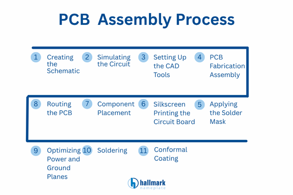
1. Creating the Schematic
The design process begins with creating a schematic, a blueprint that maps out all the electrical connections between components. Engineers use CAD tools to place symbols representing resistors, capacitors, ICs, and other essential parts, ensuring they are logically arranged for optimal function. These connections, known as “nets,” dictate how signals will flow through the board.
2. Simulating the Circuit
Before moving to physical design, engineers run simulations to test the circuit’s functionality. Using tools like SPICE, they analyze potential issues such as voltage fluctuations, signal interference, and component limitations. Identifying errors at this stage helps avoid costly revisions later in the process.
3. Setting Up the CAD Tools
Once the schematic is validated, designers configure the PCB layout software with design rules and constraints. These settings prevent overlapping connections, ensure correct trace spacing, and optimize component placement for performance and manufacturability.
4. PCB Fabrication Assembly
PCB fabrication is a multi-step process that transforms raw materials into functional printed circuit boards. Here are the key steps:
- Etching: The process removes unwanted copper from the PCB surface using a chemical etchant to create the desired circuit pattern. This is done with a photoresist mask that defines the areas to remain intact.
- Drilling: After etching, precision drills create holes for through-hole components and to form electrical connections. These holes are then plated with copper for continuity.
- Plating: Copper is applied to the surface of the PCB to enhance conductivity and prevent corrosion, using electroplating to coat vias, holes, and traces.
5. Applying the Solder Mask
After etching and plating the desired circuitry, manufacturers apply a solder mask to protect the copper traces and pads from oxidation, as well as prevent unintended electrical connections during soldering. The application of the solder mask usually involves a liquid coating, using processes like screen printing or curtain coating.
Once applied, manufacturers cure the mask with heat or ultraviolet (UV) light to harden the material and bond it securely to the PCB surface.
6. Silkscreen Printing the Circuit Board
Next, manufacturers apply silkscreen printing to add identifying marks, component designators, and other essential information to the PCB surface. This step uses special ink that resists the harsh chemicals and temperatures involved in the PCB manufacturing process.
Silkscreen printing not only provides valuable information for assembly and troubleshooting but also adds a professional finish to the PCB.
7. Component Placement
With the layout initialized, designers position component footprints on the PCB. Placement isn’t just about fitting parts; it must also consider factors like thermal management, noise reduction, and ease of assembly. Components generating excess heat are spaced appropriately, while high-speed signals are positioned to avoid interference.
Surface Mount Technology (SMT)
SMT involves mounting components directly onto the PCB surface. This approach allows for compact, cost-efficient designs and enables highly automated assembly, making it ideal for complex circuits with small form factors. SMT components are lightweight, support high-density layouts, and generally improve electrical performance due to shorter signal paths.
Through-Hole Technology
Through-hole technology requires inserting component leads through drilled holes on the PCB and soldering them in place. While more labor-intensive, this method provides mechanical strength and durability, making it suitable for components subjected to physical stress, high temperatures, or heavy currents. Through-hole placement is often combined with SMT in hybrid designs to optimize both performance and reliability.
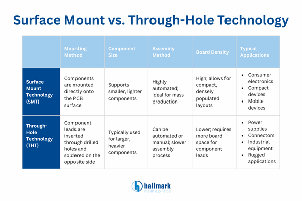
A skilled manufacturer should be proficient in both techniques and help determine the best option for your project.
8. Routing the PCB
Routing involves drawing copper traces to connect components according to the schematic. These traces must maintain proper signal integrity, avoiding issues like cross-talk and electromagnetic interference.
Modern CAD software offers automated routing features, but designers often refine them manually to ensure the best performance.
9. Optimizing Power and Ground Planes
To maintain signal stability, PCBs include dedicated power and ground planes. These layers distribute electrical currents efficiently, reducing noise and improving circuit reliability.
Designers must ensure uninterrupted return paths to prevent voltage fluctuations that could disrupt operation.
10. Soldering
Soldering is a critical step in PCB assembly, creating the electrical and mechanical connections between components and the board. Choosing the right soldering technique depends on the board design, component type, production volume, and precision requirements.
There are two primary soldering methods commonly used in PCB manufacturing.
Wave Soldering
Wave soldering is a traditional, high-throughput method where the entire PCB passes over a molten wave of solder. As the board contacts the solder wave, all exposed metal pads and component leads are simultaneously soldered.
This technique is particularly effective for through-hole components and large surface-mount parts, making it a popular choice for boards with mixed technologies.
Advantages:
- Efficient for medium- to high-volume production
- Reliable for the mechanical strength of through-hole components
- Cost-effective for simpler board designs
Disadvantages:
- Less precise for densely packed components
- Can cause solder bridges on fine-pitch parts
- Not ideal for small or delicate SMT components
Selective Soldering
Selective soldering is a more precise, modern approach, using a controlled solder nozzle or bubble to join specific components individually. This method is ideal for densely populated PCBs, hybrid assemblies, or boards with a mix of surface-mount and through-hole parts.
Selective soldering reduces the risk of heat damage to sensitive components while maintaining strong, reliable connections.
Advantages:
- High precision for small or complex boards
- Minimizes heat exposure to surrounding components
- Reduces solder defects and rework
Disadvantages:
- Slower than wave soldering for high-volume runs
- Equipment and setup can be more expensive

Both have their advantages and disadvantages, so talk with your manufacturer about which is right for your project.
11. Conformal Coating
The final stage in PCB manufacturing is the application of a conformal coating, a thin, invisible protective layer that safeguards the board’s surface without adding noticeable thickness or weight. This coating significantly enhances the reliability, durability, and lifespan of the PCB.
They help prevent damage from:
- Acids
- Bases
- Corrosion
- Salt
- Moisture and condensation
- Various industrial solvents
By sealing the board against environmental contaminants, conformal coating ensures the PCB continues to perform as intended, even in demanding conditions.
Reasons Your PCB Isn’t Working
When a PCB fails, the root cause often traces back to issues in design, manufacturing, handling, or component performance. Understanding the most common failure points can help engineers diagnose problems faster and prevent costly rework in future builds.
Below are some of the leading causes of PCB malfunction.
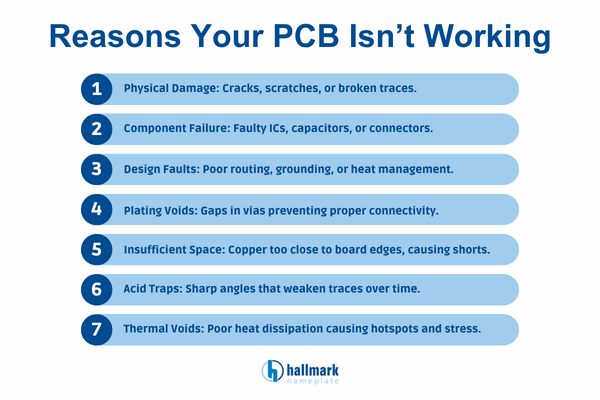
Physical Damage
Cracks, scratches, lifted pads, or broken traces can occur during assembly, handling, or installation. Even minor damage can interrupt signal flow or create intermittent failures that are difficult to trace.
Component Failure
A PCB is only as reliable as its components. Faulty capacitors, ICs, or connectors, whether from manufacturing defects, improper soldering, age, or heat stress, can cause the entire board to malfunction.
Design Faults
Improper trace routing, poor grounding, inadequate heat management, or incorrect component placement can lead to performance issues, short circuits, or total system failure. Many PCB problems can be prevented with a robust design review and DFM (Design for Manufacturability) checks.
Plating Voids
Voids in the plated through-holes or vias prevent reliable electrical connectivity between layers. These gaps weaken signal pathways, often resulting in intermittent or complete circuit failure.
Insufficient Space
When the copper layer is routed too close to the board edge, it increases the risk of shorts, delamination, and structural failure, especially during depanelization or in high-vibration environments.
Acid Traps
Sharp trace angles can trap etching chemicals during manufacturing, potentially eroding copper over time. This leads to weakened traces, shorts, or open circuits, especially in high-voltage or harsh operating environments.
Thermal Voids
Inadequate solder or poor heat dissipation around thermal vias and pads can create hot spots that stress components. These thermal voids often lead to premature component failure or intermittent issues under load.
Testing the PCB
Finally, rigorous testing ensures the board functions correctly and reliably. This ensures that the PCB functions correctly and reliably before it is integrated into the final product.
The testing process involves a series of comprehensive checks and evaluations to verify the integrity of the PCB’s design and functionality.
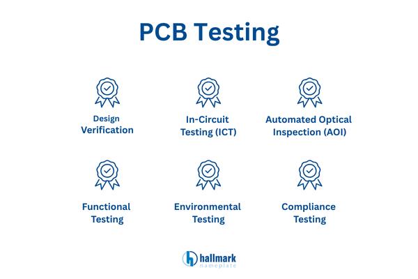
1. Design Verification
Before a PCB is physically manufactured, design verification ensures that it meets all required specifications. Using simulation tools, engineers can model how the PCB will behave under various conditions, testing aspects such as power distribution, signal integrity, and thermal performance.
This step helps identify potential design flaws before fabrication, reducing the risk of expensive rework.
2. In-Circuit Testing (ICT)
In-circuit testing is a fundamental process that checks the electrical integrity of the PCB. Using a specialized test fixture with probes, ICT identifies open circuits, short circuits, incorrect component values, and soldering defects.
This method allows manufacturers to catch errors early, ensuring that all connections are properly formed before the board moves to the next stage.
3. Automated Optical Inspection (AOI)
Automated Optical Inspection (AOI) uses high-resolution cameras and advanced imaging technology to scan the PCB for physical defects. This includes issues such as misaligned or missing components, soldering inconsistencies, and board contamination.
AOI is especially useful for identifying errors in high-density PCBs where manual inspection would be time-consuming and less accurate.
4. Functional Testing
Functional testing evaluates the PCB’s performance under actual working conditions. This test simulates the electrical load and functionality of the board, verifying that it operates as intended.
Engineers check for signal integrity, power fluctuations, and processing errors, ensuring that the board is ready for integration into the final product.
5. Environmental Testing
To ensure the PCB can withstand varied operating environments, manufacturers subject the boards to extreme conditions such as:
- Temperature Testing: PCBs are exposed to both high and low temperatures to check for thermal expansion and contraction effects.
- Humidity Testing: These tests evaluate the PCB’s resistance to corrosion and degradation in high-moisture environments.
- Vibration and Shock Testing: Simulating mechanical stress ensures the PCB can endure physical shocks and vibrations, crucial for automotive and aerospace applications.
6. Compliance Testing
Regulatory compliance is essential for PCBs used in medical, automotive, aerospace, and consumer electronics. Compliance testing ensures that the board meets safety, electromagnetic compatibility (EMC), and industry regulations, such as:
- IPC Standards (Association Connecting Electronics Industries) for PCB manufacturing quality.
- RoHS (Restriction of Hazardous Substances Directive) for lead-free and environmentally friendly production.
- UL Certification for fire safety and durability requirements.
Overall, the PCB manufacturing process is a complex yet highly precise operation that requires careful attention to detail at every step. By following established procedures and utilizing advanced manufacturing techniques, PCB manufacturers can produce high-quality printed circuit boards that meet the demanding requirements of modern electronic devices.
Applications of PCBs
PCBs power the technology we rely on every day. Their versatility, compact design, and reliability make them essential across a wide range of industries, from lifesaving medical devices to advanced aerospace systems.
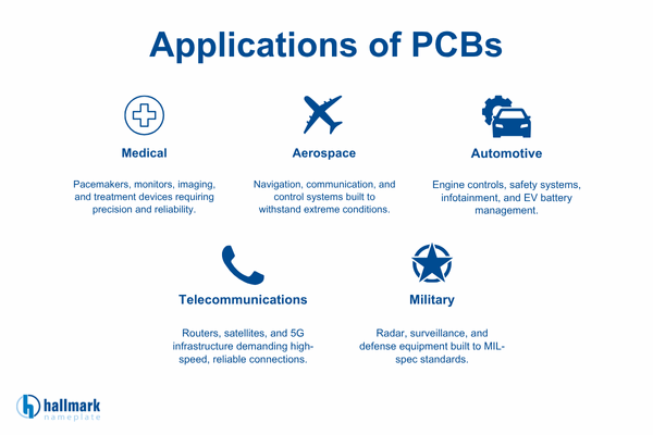
Medical
Medical-grade PCBs are used in diagnostic, monitoring, and treatment equipment where accuracy and reliability are critical. You’ll find PCBs in devices such as pacemakers, imaging systems, infusion pumps, and portable medical monitors, applications where failure is not an option.
Aerospace
In aerospace applications, PCBs must withstand extreme temperatures, vibration, and changing atmospheric conditions. They are commonly integrated into navigation systems, communication modules, control instrumentation, and flight computers, where high performance and durability are mandatory.
Automotive
Modern vehicles rely heavily on PCBs to support safety features, engine controls, infotainment systems, and advanced driver-assistance technologies. From sensors and dashboards to EV battery management systems, PCBs enable smarter, more efficient, and more connected driving experiences.
Telecommunications
PCBs are at the core of global connectivity. They help drive the infrastructure behind wireless networks, routers, satellites, and communication towers. With the rise of 5G and IoT, telecom demands PCBs with exceptional signal integrity and speed.
Military
Military and defense electronics require rugged PCBs engineered to perform in mission-critical environments. These boards are used in radar systems, communication equipment, surveillance technology, and weapons control systems, often designed to meet strict MIL-spec standards for reliability and security.
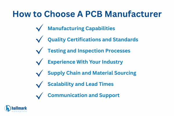
How to Choose A PCB Manufacturer
Selecting the right PCB manufacturer is one of the most important decisions you’ll make in your product development process. The right partner will deliver high-quality boards, reduce production risks, and ensure your design moves smoothly from prototype to full-scale production.
When evaluating PCB manufacturers, consider the following factors:
Manufacturing Capabilities
Look for a supplier whose capabilities match your technical requirements. Confirm they can handle your board type (rigid, flex, rigid-flex, HDI), layer count, tolerances, copper weight, controlled impedance, and any specialized materials you need.
Quality Certifications and Standards
Reputable PCB manufacturers follow strict quality and compliance standards. Prioritize partners with certifications such as ISO 9001, IPC-6012, UL, and ITAR (if applicable). These credentials indicate consistent processes, reliability, and adherence to industry requirements.
Testing and Inspection Processes
Quality PCBs require rigorous testing. Make sure the manufacturer offers AOI, flying probe, ICT, X-ray inspection, and 100% electrical testing. Thorough validation reduces the risk of defects in the field.
Experience With Your Industry
Different industries have different expectations. For example, aerospace and medical PCBs require high reliability and stricter controls, while consumer electronics may prioritize speed and cost. Choose a manufacturer with proven experience in your market.
Supply Chain and Material Sourcing
Ask how they source laminate, copper, components, and specialty materials. A reliable manufacturer will have vetted suppliers, strong inventory management, and clear traceability to help avoid counterfeit or low-grade components.
Scalability and Lead Times
Your manufacturer should support your project at every stage, from prototypes to volume production, without compromising timelines. Review their average lead times and ensure they can scale with your growth.
Communication and Support
Strong engineering support and transparent communication can save weeks of back-and-forth. Look for a partner who offers DFM feedback early, responds quickly, and collaborates, not just prints boards.
State-of-the-Art Equipment
Your manufacturer should invest in the best and latest equipment to ensure precise, high-quality production. Advanced tools support complex designs such as multi-layer, HDI, and flexible PCBs, ensuring reliable performance, faster production, and consistent adherence to industry standards.
Create A Custom Printed Circuit Board With Hallmark Nameplate
A trusted manufacturer is crucial for designing, assembling, and producing high-quality circuit boards. A skilled circuit designer can craft a printed circuit board tailored to your specific needs. Additionally, rigorous testing procedures guarantee that every aspect of the PCB functions as intended, minimizing the risk of failures in the future.
At Hallmark Nameplate, we understand the critical role that PCBs play in your products. That’s why we are committed to providing the highest quality PCB assembly services. With our expertise and dedication to excellence, we strive to empower businesses with the tools they need to succeed in today’s competitive market.
Contact us today or request a FREE quote to see how we can create the exact circuit board to fit your needs!