If you have an electronic device, it probably has a printed circuit board (PCB). These boards are responsible for the operation of electronic devices.
So what exactly are PCBs, how are they made, and why are they essential? Read our blog to find out!
Key Takeaways
- Printed circuit boards (PCBs) are the backbone of modern electronics, providing the pathways that allow power and signals to move between components.
- PCBs evolved from the 1940s to today, shifting from simple wiring replacements to complex boards that support high-density integrated circuits.
- Each PCB is built from multiple layers, including a fiberglass base, copper circuits, soldermask, and silkscreen, designed for durability, conductivity, and precision.
- High-quality PCB assembly is essential, and ITAR-certified manufacturers ensure reliable, military-grade performance for any electronic device.
What is a Printed Circuit Board?
Printed Circuit Boards are boards that connect various points together through lines and pads. They allow signals and power to connect between two physical devices. While the term “printed circuit board” is typically used, other terms to describe these include “printed wiring board” and “printed wiring card.”
Before PCBs came into existence, circuits were constructed using point-to-point wiring. This led to the failure of wire junctions and short circuits if the insulation aged or cracked. It was because of this that the need arose for a more durable unit.
PCBs also became a need as electronics became more common in consumer goods. To ensure that these everyday electronics had all of the necessary components, the size and manufacturing costs needed to be reduced.
History of the Printed Circuit Board
So how did PCBs come to be and transform over time?
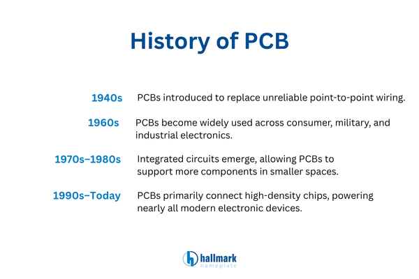
1940s – The Beginning
PCBs were first developed to connect discrete components like resistors and transistors. They replaced fragile point-to-point wiring, offering a more reliable and durable way to build circuits.
1960s – Early Adoption
While electronics still relied on discrete components, PCBs became widely used in consumer, military, and industrial devices, simplifying complex circuits.
1970s-1980s – Integrated Circuits Arrive
The emergence of integrated circuits (ICs) allowed PCBs to hold more components in a smaller space. By the 1980s, PCBs commonly featured numerous chips, improving performance and reducing size.
1990s-Today – Modern PCBs
Modern PCBs connect mostly chips instead of discrete components, supporting electronics with thousands to hundreds of millions of transistors, making them essential in virtually all devices.
What are Printed Circuit Boards Made of?
Printed Circuit Boards are composed of multiple layers, each designed to serve a specific purpose in ensuring the board’s structural integrity, electrical functionality, and durability.
Here’s a closer look at each component.
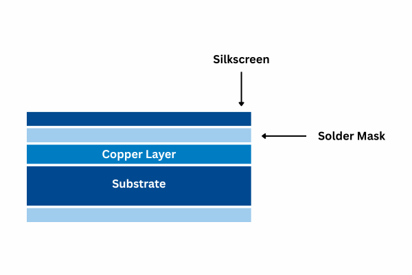
1. Substrate (Base Material)
The substrate is the foundational layer of a PCB and provides mechanical support to all other layers. The choice of substrate affects the PCB’s durability, heat tolerance, and electrical performance.
FR-4
The most common substrate material is fiberglass, historically designated as FR-4, which stands for “Flame Retardant 4.”
FR-4 is a woven fiberglass that has been treated to resist heat and combustion, making it ideal for electronic applications.
Alternative Materials
Other materials include:
- Polyimide for flexible boards
- Phenolic resin for lower-cost applications
- Ceramic for high-performance and high-temperature environments
2. Copper Layer
Laminated onto the substrate is a thin copper foil, which forms the conductive pathways of the PCB. Copper allows electricity to flow between different components, enabling the board to function as intended.
The copper can be found as a single layer on simpler PCBs or as multiple layers in more complex boards, which are connected via plated-through holes or vias.
The thickness of the copper layer can vary depending on the current requirements, typically ranging from 0.5 oz to 2 oz per square foot.
3. Soldermask Layer
The soldermask layer is applied over the copper to protect it from oxidation and prevent accidental electrical shorts. It is typically made from a polymer-based material and comes in various colors, though green is most common.
This layer ensures that solder adheres only to the intended pads during assembly, reducing the risk of bridging or unwanted connections. In addition to insulation, soldermask adds a degree of physical protection to the delicate copper traces, increasing the PCB’s durability.
4. Silkscreen Layer
The top layer of a PCB is the silkscreen, which provides visual markers such as letters, numbers, symbols, logos, and component identifiers.
Silkscreen is usually printed using epoxy ink and helps technicians and engineers identify where components should be placed or replaced. Beyond assembly guidance, the silkscreen contributes to quality control and maintenance by making boards easier to troubleshoot.
5. Additional Layers (Optional)
Advanced PCBs may include extra layers like:
- Prepreg layers (insulating layers that bond copper sheets together)
- Copper planes for power or ground distribution
- Specialized coatings, like conformal coatings, for added environmental protection.
Flexible and rigid-flex PCBs may also incorporate polyimide or other bendable materials to allow the board to twist or fold without breaking the circuitry.
By carefully combining these layers, PCBs achieve a balance of mechanical strength, electrical conductivity, and resistance to heat, moisture, and mechanical stress, all of which are crucial for modern electronic devices to function reliably.
What are Etched Circuits?
Printed circuits are essentially etched circuits, created by removing unwanted copper to form precise electrical pathways. These circuits can range from simple single-layer designs to complex multi-layer boards.
1. Applying the Copper and Photoresist
Each PCB layer starts with copper foil laminated onto a fiberglass or plastic base.
This copper is then coated with photoresist, a light-sensitive material that becomes resistant to chemicals when exposed to light.
2. Exposing the Circuit Pattern
A negative image of the circuit design is placed over the board. Light shines through this pattern onto the photoresist, hardening the areas that represent the desired circuit paths.
3. Etching the Unwanted Copper
Any photoresist that didn’t harden is removed during an acid bath, which also washes away the exposed copper underneath, creating the finished circuit traces.
The hardened areas remain intact, forming clean, defined copper pathways.
4. Final Layer Bonding
Once each layer is etched, the layers are aligned and glued together to build the final PCB structure, especially in multi-layer board designs.
Why Hallmark Nameplate?
The functionality and construction of electronics have developed dramatically over the years. As technology has advanced, the need for printed circuit boards has increased. Even after PCBs were invented, most electronics featured more discrete components than chips.
However, as manufacturers attempt to make smaller and less expensive devices, chips are more common than discrete components, making PCBs that much more important.
Hallmark Nameplate is a company that features experienced professionals when it comes to assembling PCBs. Our services include PCB assembly, testing, PCB encapsulation, prototype PCB assembly, and PCB engineering.
As an ITAR-certified producer of PCBs and a member of the Special Graphic Imaging Association (SGIA), Hallmark Nameplate holds itself to a high standard, producing military-grade products.
When having PCBs manufactured or assembled, it is imperative that they are done to the highest quality to ensure maximum functionality of electronic devices. If you’re in need of PCB assembly services, get in touch today!