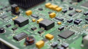
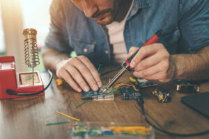
Printed Circuit Boards (PCBs) are the backbone of modern electronics. They contain intricate networks of electrical connections that enable the smooth functioning of devices ranging from cell phones to computers. But, circuit board repair techniques are not typically at the forefront of your mind when you buy a piece of technology.
Unfortunately, these crucial PCB components are not immune to damage. When one fails, it can be a frustrating and costly experience for businesses and individuals alike. The good thing is repairing a PCB is often a viable solution that can save you both time and money.
In this blog, we will delve into the world of printed circuit board repair, exploring the various types of damage that can occur and the tools and techniques used for repair. Whether you’re a professional electronics technician or a hobbyist, this guide will provide you with valuable insights into the specialty of circuit board repair.
7 Reasons Your Circuit Board Isn’t Working
1.) Physical Damage
A printed circuit board contains conductive pathways etched onto its surface. These pathways carry signals and power between electronic components mounted on the board. Physical damage to a PCB can cause it to stop working by interrupting these conductive pathways or damaging the electronic components.
For example, if the board is bent or cracked, it can cause the pathways to break or become disconnected from the components. Similarly, exposure to moisture, heat, or chemicals can corrode or damage the conductive pathways or the components themselves.
Excessive vibration or shock can also dislodge components or cause them to break loose from the board, disrupting the circuit’s operation. This is why it is important to handle and store PCBs carefully to avoid physical damage and ensure its longevity.
2.) Component Failure
There are a few common components of a circuit board that we should differentiate.
- Batteries provide a source of electrical power.
- Capacitors store electrical charge to ensure even distribution.
- Copper traces are the embedded copper pathways on a board that facilitate the flow of electrical current.
- Diodes control the direction of electrical current.
- Inductors store electrical current as an electromagnetic field.
- Light-emitting diodes (LEDs) enable one-way current flow and light up when there is current present.
- Resistors slow down the electrical current.
- Switches can allow or block the flow of current depending on whether they are open or closed.
- Transistors amplify the electrical charge.
A failure of any of these components can cause the PCB to stop working. Electronic components are susceptible to a variety of failure modes, including electrical overstress, thermal stress, mechanical stress, and aging.
Electrical overstress occurs when a voltage or current exceeds the component’s specifications, which causes it to fail. Thermal stress occurs when the component operates at a temperature outside its specified range. Mechanical stress can occur during assembly, shipping, or use, causing components to crack or become dislodged.
Finally, aging can cause components to degrade over time, eventually leading to failure. Therefore, it is important to use high-quality components that are specified for the application and to ensure that they are properly installed and tested to minimize the risk of failure.
3.) Design Faults
While some aspects of PCB failure can be attributed to user error, some boards just simply have design faults. PCBs have traces to provide connections between components on the board which allow signals and power to flow through the circuit. Any design fault that interrupts or distorts these connections can cause the PCB to stop working, leading to malfunctions or complete device failure.
One common design fault that can cause a PCB to stop working is incorrect routing of traces. When the traces are not routed properly, it can lead to interference between signals or cause high impedance points that interrupt proper signal transmission.
For example, if two traces that carry different signals are routed too closely together, the signals may interfere with each other. This can lead to noise or even signal loss. Similarly, if a trace is too long or has too many bends, it can result in a high impedance point and reduce the signal strength.
4.) Plating Voids
Plating voids are another potential cause of PCB failures. The process of plating is used to create a conductive layer on a PCB’s surface, typically made of copper, which forms the traces and pads that connect the components.
Voids are small, empty spaces or gaps that can form in the conductive layer during the plating process. These voids can cause the PCB to fail in several ways. For example, they can lead to incomplete electrical connections or even complete breaks in the circuit. They can also result in corrosion and degradation of the PCB over time. Plating voids can be caused by various factors, including inadequate cleaning of the PCB surface, poor plating solution quality, or incorrect plating process parameters.
5.) Not Enough Space Between Copper and Board Edge
Insufficient copper-to-edge clearance is a design issue that can cause problems in PCB manufacturing and assembly. The copper-to-edge clearance refers to the distance between the edge of the copper feature, such as a trace or pad, and the edge of the PCB.
If this clearance is too small, it can result in manufacturing and assembly issues, such as the copper feature being cut or damaged during the PCB cutting process or causing shorts when the PCB is installed in its final product. The recommended copper-to-edge clearance depends on factors like the PCB manufacturer’s capability and the complexity of the board.
6.) Acid Traps
Acid traps can occur when the etchant solution becomes trapped in acute angles of the board and is unable to escape. As a result, the acid continues to eat away at the copper, which can cause the copper traces or pads to break, leading to a complete PCB failure.
Acid traps can be prevented by careful design and inspection of the PCB before manufacturing. Designers can avoid the issue by designing boards with minimal cavities or holes and by ensuring that there is enough clearance between the copper features and the edges of any holes or cavities. Additionally, manufacturers can use inspection processes to detect any acid traps and make the necessary circuit board repair before the PCB is completed.
7.) Thermal Voids
Thermal voids are a common issue that can cause PCB failure in high-temperature applications. It is a cavity or gap in the copper feature or via that is caused by the expansion and contraction of trapped gasses within the PCB during thermal cycling. These voids can lead to a reduction in the thermal conductivity of the PCB. They can also increase the temperature of the components.
Over time, the increased temperature can lead to device failure or degradation. Thermal voids can be prevented by using proper design techniques and selecting appropriate materials. For example, using smaller copper features or choosing materials with a low coefficient of thermal expansion can help to reduce the formation of thermal voids.
Troubleshooting Circuit Board Repair
Now that you know some of the main causes of PCB failure, it’s worth it to learn how to troubleshoot circuit board repair. But before you can begin troubleshooting the repair process, you need to identify the root cause of the problem.
First, inspect the PCB for any physical damage. This can be cracked or broken components, burned traces or pads, or signs of corrosion. Next, check the power supply and other components to ensure that they are working correctly. You can use a multimeter or other testing equipment to check the resistance, continuity, and voltage of the various components.
If you identify any faulty components, replace them with new ones. If you cannot find any physical damage or faulty components, it’s possible that the PCB has a design or manufacturing issue. In this case, you may need to consult with the manufacturer or a PCB design expert to identify the problem and develop a solution.
Choose a Trusted Manufacturer For Your PCB
At Hallmark Nameplate, we pride ourselves in producing only the highest quality electronic assemblies and membrane switches for various industries, including medical, aerospace, telecommunications, and automotive.
We use state-of-the-art equipment and technologies to thoroughly test that each PCB assembly meets the client’s requirements and standards. Our experienced team of technicians can assist with design, testing, and troubleshooting to ensure that the final product meets your expectations.
Contact us today or request a FREE quote to see how we can help you with your circuit board repair!