

Every electronic device you rely on, from the diagnostic monitor in an operating room to the avionics panel inside a cockpit, starts as a bare printed circuit board. Turning that blank substrate into a functioning electronic assembly requires a precise, multi-stage manufacturing process where each step builds on the last.
Understanding the PCB assembly process helps engineering managers, procurement teams, and product designers evaluate potential manufacturing partners, anticipate lead times, and make informed decisions about component selection and assembly methods.
This guide walks through every major stage of the PCB manufacturing process, from initial design review through final quality testing, with a practical comparison of Surface Mount Technology (SMT) and Through-Hole Technology (THT) along the way. For a broader overview of electronic assembly types and PCB fundamentals, see our Complete Guide to PCB and Electronic Assembly.
Key Takeaways:
- The PCB assembly process follows a defined sequence from DFM review and solder paste application through component placement, soldering, inspection, and final testing, where each stage builds on the last and skipping steps introduces compounding risk.
- SMT and through-hole technology serve different purposes: SMT enables high-density, automated placement for compact designs, while THT delivers the mechanical strength required for defense, medical, and high-vibration applications. Many modern assemblies use both.
- Effective PCB manufacturers embed quality control at multiple stages — solder paste inspection, automated optical inspection after reflow, X-ray analysis for hidden joints, and in-circuit plus functional testing — before a board ships.
- Certifications and registrations such as ISO 9001:2015, ISO 13485:2016, ITAR registration, and applicable UL programs may be important qualification factors depending on the industry, product, and program requirements.
- Working with a single U.S.-based manufacturer from prototype through production eliminates process translation errors between vendors, simplifies supply chain oversight, and reduces time-to-market.
What Is PCB Assembly?
PCB assembly, commonly abbreviated as PCBA, is the process of soldering and mounting electronic components onto a fabricated printed circuit board. It transforms a bare board with etched copper traces into a fully functional circuit capable of powering a finished product.
PCB assembly is distinct from PCB fabrication.
Fabrication creates the physical board itself:
- Etching copper pathways
- Drilling holes
- Applying solder mask
- Printing the silkscreen layer
Assembly is what comes next: populating that board with resistors, capacitors, integrated circuits, connectors, and other components, then soldering them into place.
The assembly process can use Surface Mount Technology (SMT), Through-Hole Technology (THT), or a combination of both. This depends on the design requirements, mechanical demands, and production volume of the project.
Although PCB fabrication and PCB assembly are separate stages, both are part of the broader PCB manufacturing process.
The PCB Assembly Process: Step by Step
While specific workflows vary between manufacturers, the core PCB assembly process follows a consistent sequence. Here is how a bare board becomes a finished electronic assembly.

Step 1: Design Review and DFM Analysis
Before any components touch the board, the manufacturer reviews your design files, typically Gerber files, a bill of materials (BOM), and assembly drawings.
A Design for Manufacturability (DFM) analysis checks for potential production issues:
- Component spacing conflicts
- Pad size mismatches
- Tombstoning risks
- Thermal relief adequacy
Catching these issues before production starts prevents costly rework and delays. A thorough DFM review is often one of the clearest indicators of a capable contract manufacturer.
Step 2: Solder Paste Application

For SMT assemblies, the process begins by applying solder paste to the bare board. A stainless steel stencil is aligned over the PCB, and solder paste, a mixture of tiny solder spheres suspended in flux, is deposited onto the exposed pads through the stencil openings using a squeegee.
Paste volume and alignment are critical. Too much paste causes bridging between adjacent pads; too little creates weak or open joints. Automated stencil printers with vision alignment systems ensure consistent deposition across every board in a production run.
Step 3: Component Placement
Once solder paste is applied, the board moves to an automated pick-and-place machine. These machines use vacuum nozzles to pick surface-mount components, from transistors and capacitors to transformers, and place them onto the pasted pads at high speed.
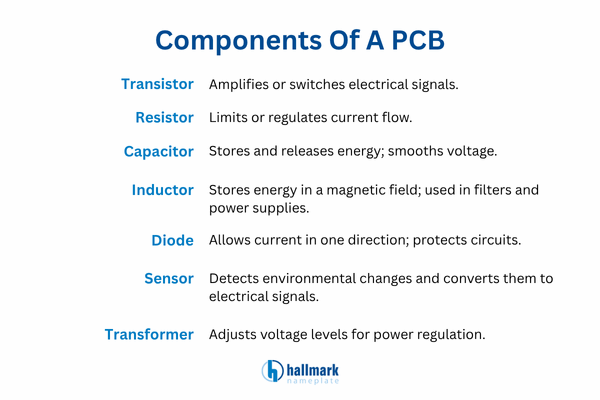
Modern pick-and-place systems can position thousands of components per hour with placement accuracy measured in microns. At Hallmark Nameplate, our electronic assembly line uses Samsung SM482, SM421, and CP-40 placement systems for reliable, high-precision SMT component placement.
Step 4: Reflow Soldering (SMT)
After component placement, the board enters a reflow oven. The oven follows a carefully controlled thermal profile with distinct zones: preheat, thermal soak, reflow (peak), and cooling.
During the reflow zone, temperatures rise high enough to melt the solder paste and form permanent electrical and mechanical bonds between the components and the board.
The thermal profile is calibrated for each board design to prevent damage to heat-sensitive components while ensuring every joint reaches the proper temperature. Lead-free soldering processes, required for RoHS Compliant assemblies, use higher peak temperatures than traditional leaded solder processes.

Step 5: Through-Hole Component Insertion
For boards that require through-hole components, common in defense, medical, and high-vibration applications, leaded components are inserted through drilled holes in the PCB either manually or with automated insertion equipment.
Through-hole components generally provide greater mechanical retention for components exposed to physical stress or vibration. This makes them the preferred choice for connectors, transformers, electrolytic capacitors, and other components that experience physical stress or need to withstand harsh operating environments.
Step 6: Wave or Selective Soldering
Once through-hole components are inserted, the board passes through a wave or selective soldering process to form the solder joints.

Wave Soldering
Wave soldering passes the entire board over a standing wave of molten solder. Every exposed lead and pad contacts the solder simultaneously. This method is efficient for boards with all through-hole components or boards with large surface-mount parts on one side.
Selective Soldering
Selective soldering uses a programmable nozzle to apply solder to individual joints or small groups of joints. This approach is increasingly preferred for densely populated boards where wave soldering would risk damaging adjacent SMT components. At Hallmark Nameplate, we use an Ersa SMARTFLOW 2020 selective soldering system for precise, programmable through-hole soldering.
Step 7: Automated Optical Inspection (AOI)
After soldering, every board undergoes Automated Optical Inspection. High-resolution cameras scan the board and compare it against the original design data. Then it flags defects such as missing components, misaligned parts, solder bridges, insufficient solder joints, and incorrect component polarity.
AOI catches many common assembly defects early in the process before additional value is added. This reduces rework costs and prevents defective boards from reaching downstream testing stages.
Step 8: X-Ray Inspection
For assemblies that include components with hidden solder joints, such as Ball Grid Arrays (BGAs) or Quad Flat No-Lead (QFN) packages, X-ray inspection is used to verify solder quality beneath the component body where optical inspection cannot see.
X-ray analysis reveals voids, bridging, head-in-pillow defects, and insufficient wetting that would otherwise go undetected until functional testing or field failure.
Step 9: Conformal Coating
For boards destined for harsh operating environments such as aerospace, military, marine, outdoor industrial, a conformal coating may be applied after assembly. This thin, transparent protective layer conforms to the board’s surface contours and shields components and solder joints from moisture, dust, chemicals, salt spray, and temperature extremes.
Conformal coatings add protection without meaningfully increasing board thickness or weight, and they do not obscure indicator lights or printed markings on the board surface.
Step 10: Functional and Environmental Testing
The final stage of the PCB assembly process is comprehensive testing to verify that every board performs as designed under real-world conditions.
- In-Circuit Testing (ICT) uses a bed-of-nails fixture to probe individual components and verify correct values, orientation, and connectivity.
- Functional Testing powers the board and simulates real operating conditions to confirm the assembly performs its intended function.
- Environmental Testing subjects boards to temperature cycling, humidity exposure, thermal shock, and vibration to validate durability under the conditions they will face in the field.
At Hallmark Nameplate, our testing infrastructure includes seven dedicated workstations equipped with SPEA 3030 in-circuit testers, YesTech FX Series AOI systems, and Nordson Dage X-ray inspection, plus environmental chambers for temperature, humidity, thermal shock, and vibration testing.
SMT vs. THT: Choosing the Right Assembly Method
One of the most important decisions in the PCB assembly process is selecting between Surface Mount Technology and Through-Hole Technology or, in many cases, using both in a mixed-technology assembly.
The table below summarizes the key differences:
| Attribute | SMT (Surface Mount) | THT (Through-Hole) |
|---|---|---|
| Component Placement | Mounted directly on board surface | Inserted through drilled holes |
| Solder Method | Solder paste + reflow oven | Wave or selective soldering |
| Board Density | Higher — components on both sides | Lower — typically single-side |
| Mechanical Strength | Adequate for most standard applications | Superior — stronger solder joints |
| Automation Level | Highly automatable, faster throughput | More manual, slower throughput |
| Cost at Volume | Lower per-unit cost at scale | Higher due to process complexity |
| Component Size | Smaller components (0201 and up) | Larger leaded components |
| Ideal Applications | Consumer, telecom, compact assemblies | Defense, medical, high-vibration |
| Hallmark Capability | Samsung SM482, SM421, CP-40 lines | Wave & selective (Ersa SMARTFLOW 2020) |
Surface Mount Technology (SMT)
Because components sit on the surface rather than passing through it, SMT enables placement on both sides of the board for higher density in a smaller footprint. The process is highly automatable, which drives faster throughput and lower per-unit costs at scale, making it the standard for consumer electronics, telecom, and compact assemblies.
Through-Hole Technology (THT)
THT creates a stronger mechanical bond, which is why connectors, transformers, power components, and parts exposed to vibration or thermal cycling are still assembled using through-hole methods. Certain defense, aerospace, medical, and high-vibration applications may use THT for components requiring additional mechanical strength.
Mixed Technology
Many modern PCB designs use mixed technology:
- SMT for the majority of components where density and speed are priorities.
- Combined with through-hole placement for connectors, power components, or parts that must withstand mechanical stress.
A capable contract manufacturer should be proficient in both methods and help you determine the optimal approach for your application.
Quality Control Throughout the PCB Assembly Process
Quality is not a single checkpoint at the end of the assembly line; it is built into every stage of the process. Effective PCB manufacturers embed inspection and verification at multiple points rather than relying on end-of-line testing alone.
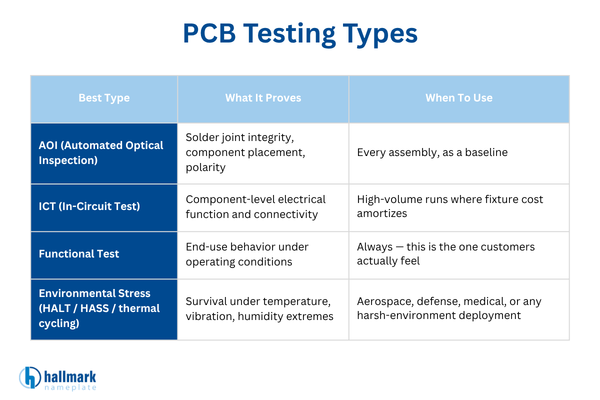
- Pre-production: DFM analysis, solder paste inspection (SPI), and first-article verification before full production begins.
- In-process: AOI after reflow, X-ray for hidden joints, visual inspection at critical hand-assembly stages.
- Post-assembly: In-circuit testing, functional testing, and environmental stress screening.
Industry certifications provide an external validation layer. Look for manufacturers certified to ISO 9001:2015 for general quality management and ISO 13485:2016 for medical device manufacturing. For defense and aerospace programs, ITAR registration, applicable UL programs, and other qualifications may be required depending on the specific program.
What to Look for in a PCB Assembly Partner
Not every contract manufacturer is equipped to handle every project. When evaluating a PCB assembly partner, consider the following.
Assembly Capabilities
Can they handle SMT, THT, and mixed-technology assemblies on the same production line? Do they have the pick-and-place systems, soldering equipment, and component handling capacity for your specific board complexity — not just a general capability claim on a website?
Certifications
Quality certifications, regulatory registrations, and compliance capabilities may include ISO 9001:2015, ISO 13485:2016, ITAR registration, applicable UL programs, and RoHS-compliant manufacturing. They determine whether a manufacturer can bid on aerospace, medical, and defense programs. Ask for current certificates, not just logos.
Testing infrastructure
AOI, X-ray, in-circuit testing, and environmental testing should all be available in-house, not outsourced to a third party. When testing is under the same roof as assembly, defect feedback loops are tighter and turnaround on rework is faster.
Prototype-to-Production Scalability
The best partners can take you from a single prototype through full production runs without changing vendors. Switching manufacturers between prototyping and production introduces process translation errors that often do not surface until boards are in the field.
U.S.-Based Manufacturing
For defense, aerospace, and medical programs, Domestic manufacturing with appropriate ITAR controls can simplify export-compliance management and supply-chain oversight for applicable programs. It also reduces lead time variability compared to offshore sourcing, where shipping delays and customs holds can push timelines by weeks.
Partner With a Proven PCB Assembly Team
Hallmark Nameplate provides full-service PCB manufacturing and electronic assembly services from our 30,000-square-foot facility in Mount Dora, Florida. With over 60 years of production experience and certifications including ISO 9001:2015, ISO 13485:2016, ITAR Registered, UL Listed, and RoHS Compliant, we serve aerospace, medical, defense, and industrial OEMs nationwide.
If you are ready to take the first step, request a PCB Assembly quote.
Or if you’d like to see the quality of our work firsthand, request a FREE Sample Kit to evaluate materials, finishes, and build quality before committing to a production order.
Frequently Asked Questions About the PCB Assembly Process
What is the PCB assembly process?
The PCB assembly process is the multi-step manufacturing workflow that transforms a bare printed circuit board into a functioning electronic assembly. It includes solder paste application, component placement, reflow or wave/selective soldering, optical and X-ray inspection, conformal coating, and functional testing.
What is the difference between PCB fabrication and PCB assembly?
PCB fabrication creates the physical board, etching copper traces, drilling holes, applying solder mask, and printing the silkscreen. PCB assembly is the subsequent process of mounting and soldering electronic components onto that fabricated board to create a working circuit.
What is the difference between SMT and through-hole assembly?
Surface Mount Technology (SMT) places components directly onto the board surface and uses reflow soldering. Through-Hole Technology (THT) inserts component leads through drilled holes and uses wave or selective soldering. SMT enables higher component density and faster production; THT provides stronger mechanical bonds for high-stress applications.
How long does PCB assembly take?
Lead times vary by board complexity, component availability, and production volume. Prototype runs can often be completed within days, while production orders typically require one to several weeks. Your manufacturer should provide a specific timeline based on your design files and BOM.
What quality certifications should a PCB assembler have?
Look for ISO 9001:2015 for quality management, ISO 13485:2016 for medical device manufacturing, ITAR Registered status for defense and aerospace work, and UL Listed certification. RoHS Compliant manufacturing is required for products entering European markets and increasingly expected across all sectors.
What is conformal coating and when is it needed?
Manufacturers apply conformal coating, a thin protective layer, to finished PCB assemblies to shield them from moisture, dust, chemicals, and temperature extremes. Aerospace, military, marine, outdoor, and industrial deployments typically require it wherever environmental exposure could compromise reliability.
Can one manufacturer handle both prototyping and production?
Yes. Working with a single manufacturer from prototype through production ensures continuity in quality, eliminates the risk of process translation errors between vendors, and typically results in faster time-to-market. Hallmark Nameplate supports the full lifecycle from prototype assembly through volume production at our U.S. facility.