Your prototyping PCB run is where the project either de-risks or derails, and most engineering teams feel that pressure by revision three.
That’s why choosing the wrong manufacturer can make or break the project and your sanity.
Here’s what this guide covers: how to structure PCB prototyping to avoid rework, what PCB testing actually proves versus what it only suggests, and where most assembly programs lose weeks they can’t get back.
Key Takeaways:
- Prototype spins set the economics for the whole program — flaws caught at prototype cost cents; the same flaws in production cost thousands.
- PCB testing is four disciplines, not one — AOI, ICT, functional, and environmental stress. The right mix depends on volume, environment, and compliance.
- Your regulatory environment shapes the test plan from day one — aerospace, medical, and defense programs can’t retrofit compliance at the end of a build.
- DFM review before quoting separates partners from vendors — if a supplier quotes exactly what you sent, budget for a second prototype.
Why PCB Prototyping Decides the Cost Curve
Here’s the truth nobody in the pitch meeting tells you: the first prototyping PCB spin sets the economics for the entire program.
Every design flaw you catch in prototyping costs cents. Every flaw you miss costs dollars in production and causes five-figure delays in the field.
The three failure points that derail most prototype runs
- DFM gaps — designs released to fab without a manufacturability review, producing yield losses that the engineer blames on the shop floor.
- Incomplete test coverage — a PCB testing plan that validates function but ignores environmental or compliance stress.
- Unclear documentation trail — prototypes that move to production without a traceable BOM, ECN, or revision control, triggering audit findings later.
Want to know the painful part? All three are preventable in the quote stage.
5 Main Benefits of PCB Prototyping
Here’s what a disciplined prototyping PCB run actually buys you, beyond the board itself.
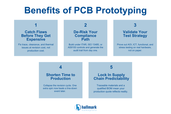
1. Catch Design Flaws Before They Get Expensive
Prototyping surfaces trace, clearance, and thermal issues while fixes cost a revision instead of a production run. That’s the single biggest ROI lever in any electronic assembly program.
2. De-Risk Your Compliance Path
A prototype built under ITAR, ISO 13485, or AS9100-aligned controls generates the documentation trail your end customer’s auditor will ask for. Skip this step, and you’re backfilling paperwork under deadline pressure.
3. Validate Test Strategy, Not Just Design
Prototyping lets you prove out AOI, ICT, functional, and environmental stress testing on the actual board, so your production test plan is calibrated, not theoretical.
4. Shorten Your Time to Production
Catching issues early collapses the revision cycle, which is where most programs lose weeks. One extra prototype spin now beats a field failure or a line-down event later.
5. Lock in Supply Chain Predictability
A documented prototype with traceable materials and a qualified BOM means your production quote reflects reality. No surprise component swaps, no “we couldn’t source that,” no margin erosion after PO.
What a Disciplined Prototyping PCB Process Looks Like
A prototype isn’t a cheap production run. It’s a structured experiment designed to answer specific questions before capital gets committed.
At Hallmark Nameplate, the prototyping PCB workflow is built around four non-negotiable stages
1. DFM and DFT Review
Before a single board is fabricated, engineering reviews your design for manufacturability (DFM) and testability (DFT).
This catches trace-width violations, pad-to-component clearance issues, and test point access problems, the quiet killers of first-article yield.
2. Controlled Build With Traceable Materials
Every prototype board is built with the same material certifications, solder profiles, and operator documentation you’d expect in a production ITAR run.
That means your prototype results actually predict production results, instead of creating a false baseline you’ll chase later.
3. First-Article Inspection
First-article inspection (FAI) validates that the physical build matches the design file before any testing begins.
Skip this step, and you’re testing noise, not performance.
4. Documented Change Control
Every revision is logged, attributed, and traceable, critical for medical and defense programs operating under ISO 13485 or ITAR.
PCB Testing: What It Proves, and What It Doesn’t
Here’s where most programs get it wrong: PCB testing isn’t one thing. It’s a stack of disciplines, each answering a different question.
Pick the wrong test for the wrong question, and you ship a board that passes QC and fails in the field.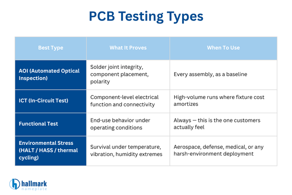
The four PCB testing disciplines that matter:
- AOI (Automated Optical Inspection)
- ICT (In-Circuit Test)
- Functional Test
- X-ray testing
- Environmental Stress (HALT / HASS / thermal cycling)
The right PCB testing protocol depends on your end application, regulatory environment, and volume.
Why Compliance Environment Shapes Your Test Plan
Here’s something procurement teams learn the expensive way: a PCB testing plan that works for consumer electronics is disqualifying for medical or defense.
Your regulatory environment isn’t a box to check at the end. It determines the entire test architecture from day one.
By industry:
- Aerospace — AS9100-aligned documentation, environmental stress testing, and full material traceability. Your PCB testing records are audit artifacts.
- Medical — ISO 13485 compliance, design history file contributions, biocompatibility considerations for any board contacting patient environments.
- Defense — ITAR-registration, controlled documentation, U.S.-only manufacturing footprint. This is where Hallmark’s Mt. Dora, FL, facility matters to your contracting officer.
- Industrial — UL-listing, RoHS-compliance, and realistic duty-cycle testing that mirrors actual field conditions.
If your supplier can’t articulate which of these apply to your program before quoting, that’s a procurement red flag.
How to Evaluate a PCB Prototyping and Testing Partner
Most RFQs get sent to five suppliers and judged on price per board. That’s the shortest path to a second prototype you didn’t budget for.
Here’s a better evaluation framework, the one your program manager will thank you for at month six. Five questions that separate serious suppliers from lowest-bid roulette:
- Will you do a DFM review before quoting, or are you quoting exactly what I sent you?
- What’s your first article yield on prototypes in my industry over the past twelve months?
- Can I see a redacted traceability record from a program comparable to mine?
- What does your test plan look like for my compliance environment, specifically?
- What’s your escalation path when a prototype reveals a design issue? Do I get an engineer or a ticket number?
If a supplier can’t answer those cleanly, you’re not buying a partner. You’re buying a vendor.
PCB Prototyping & Testing FAQs
What are the main benefits of PCB prototyping?
PCB prototyping catches design flaws before they become expensive, de-risks compliance obligations, validates your test strategy on actual hardware, shortens time to production, and locks in supply chain predictability. Catching issues at the prototype stage is typically far less expensive than addressing them in production or after deployment.
What are the four main types of PCB testing?
The four core PCB testing disciplines are Automated Optical Inspection (AOI), In-Circuit Test (ICT), Functional Test, and Environmental Stress Testing (including HALT, HASS, and thermal cycling). Each answers a different question about board quality, and the right mix depends on production volume, operating environment, and regulatory compliance requirements.
Why does the compliance environment affect a PCB testing plan?
The regulatory environment determines the entire test architecture from day one.
Aerospace programs require AS9100-aligned documentation and environmental stress testing. Medical devices require ISO 13485:2016 compliance and design history file contributions.
Defense programs require ITAR registration and U.S.-only manufacturing. Industrial applications require UL listing and RoHS compliance. A test plan built for consumer electronics is disqualifying in these regulated environments.
What is a DFM review, and why does it matter before quoting a PCB prototype?
Design for Manufacturability (DFM) review is an engineering analysis of your PCB design to identify trace-width violations, pad-to-component clearance issues, test point access problems, and other manufacturability risks before fabrication begins.
Skipping DFM review is one of the most common reasons teams need additional prototype rounds. A strong supplier should flag manufacturability risks early, not simply quote the files as submitted.
How should I evaluate a PCB prototyping and testing supplier?
Ask five questions before awarding a PCB prototype build.
- Will the supplier complete a DFM review before quoting?
- What is their first-article yield on prototypes in your specific industry over the past twelve months?
- Can they show a redacted traceability record from a comparable program?
- What does their test plan look like for your specific compliance environment?
- What is their escalation path when a prototype reveals a design issue, and will you reach an engineer or a ticket number?
What industries does Hallmark Nameplate manufacture PCB assemblies for?
Hallmark Nameplate manufactures electronic assemblies, including PCB prototyping and testing, for aerospace, medical, industrial, and defense customers. The company has operated since 1957 and holds ISO 9001:2015, ISO 13485:2016, ITAR registration, UL Listed, RoHS compliance, and 3M Preferred Converter certifications, with all manufacturing performed in Mt. Dora, Florida.
Get a High-Quality PCB
If your next prototyping PCB run is going to a fab that treats PCB testing as an afterthought, or to a supplier who can’t walk you through their DFM process before they quote, you already know how that story ends.
Hallmark Nameplate has built electronic assemblies, including prototyping PCB runs and comprehensive PCB testing, for aerospace, medical, industrial, and defense customers since 1957.
That isn’t a tagline. It’s a traceable operating record under ISO, ITAR, UL, and 3M Preferred Converter certifications, manufactured entirely in Mt. Dora, Florida.
What you get when you run a prototype through Hallmark Nameplate:
- DFM and DFT review included in the quote process, not billed as a change order
- U.S.-based engineering contact for every active program
- Test plans built around your compliance environment
- Full documentation package that survives your customer’s audit, not just ours
Request a free DFM review and prototype quote from Hallmark Nameplate. A U.S.-based engineer will review your design, flag manufacturability risks, and scope a test plan matched to your compliance environment, before you commit to a build.
Sixty-nine years of making mission-critical manufacturing boring in the best possible way. Let’s make yours boring, too.