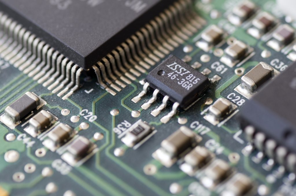
Hallmark Nameplate has an electrostatic discharge-controlled manufacturing facility to provide you with through-hole, surface mount, or mixed-PCB assembly services. You may need a PCB, or printed circuit board, for your business or product, and if you’ve come to us to make it happen, you’ve certainly come to the right place! But the best way for you to realize the true care we put into our circuit boards, it’s important to first understand exactly how they work and how that influences their function and capabilities.
The truth is that printed circuit boards are one of the key components of electronics. Here’s what you need to know about PCBs like those made at Hallmark Nameplate:
What is a printed circuit board?
While they most often go by printed circuit boards (and they go by PCBs at Hallmark Nameplate), they are also called printed wiring boards or printed wiring cards by others. Before they were invented, it took a labor-intensive process of point-to-point wiring just to create a circuit. As a result, there were frequent failures at wire junctions, and shorter circuits because wire insulations would eventually crack due to age.
An advancement that propelled the creation of PCBs into the future was wire wrapping, which is done by wrapping a small gauge wire around a post at each connector point, which resulted in a gas-tight connection. These connections are not just highly durable but proved to be much easier to change. Shortly thereafter, electronics began to make a shift from vacuum tubes and relays to more silicon and integrated circuits. This was great for production, because not only did the size of electronic components decrease exponentially, but so did the cost. The common buyer looked more and more to electronic products, which lead those looking to meet this demand to reduce the size and manufacturing costs. They began looking for better solutions, which lead to the birth of the PCB.
How do you make a printed circuit board?
To describe it in a very relatable way, a printed circuit board is made up of many layers, like a cake or a lasagna. The alternating layers of different materials are bound together with heat and adhesive, which creates a single entity.
The middle, or base layer, contains the substrate which is usually fiberglass. Having a solid core allows the PCB to be rigid and adds to its thickness. Keep in mind that there are also flexible PCBs that are built on high-temperature plastic. The thickness of the printed circuit boards can vary, and Hallmark Nameplate is very accommodating of the qualities you will need for your project.
Typically, the next layer around the substrate is thin and made of copper foil; this is laminated to the circuit board with heat and adhesive as well. Most of the time, this copper layer is applied to both sides of the substrate. One common term in the industry is a “double-sided” or “two-layer board” which refers to the number of copper layers (two) in the PCB design. The number of copper layers can be as little as one or as many as 16, or more! Another feature that varies is the thickness of each copper layer. Each ounce per square is translatable to about 35 micrometers, or 1.4 thousandths of an inch of copper thickness.
The third layer is called the solder mask layer, which provides the color of the PCB, often green. The solder mask layer is placed over the copper layer to insulate the copper traces from accidental contact with things such as other metals, solders, or conductive bits. Preventing solder jumpers is just one part of what this layer is relied on for – it also helps the user to solder to the correct places, which can be tricky or even impossible without the use of the solder mask layer. While it is often green, it is possible to have a solder mask in virtually any color, so don’t worry about the aesthetics; Hallmark Nameplate has you covered—or should we say, “colored.”
The final layer is called silkscreen, and it is usually the layer that has letters, numbers, and symbols that make for the easiest assembly possible. There are also other types of indicators that allow anyone using the printed circuit board to understand what goes where, or otherwise how to use it. Similar to the solder mask layer, the silkscreen layer is often white but can be customized with any ink color. Keep in mind, however, that it is not common to have more than one color on each PCB.
Understanding the different elements of a PCB board is helpful when deciding what exactly you need for your business. When it comes to quality, you won’t find anyone better than Hallmark Nameplate to work with you on your project, from design to completion. Contact us today to get your PCB started today!


